
PCB Assembly + Electronic Device Manufacturing
SMT + DIP + final assembly under one roof. Ideal for small-to-mid IoT production runs.
Gallery
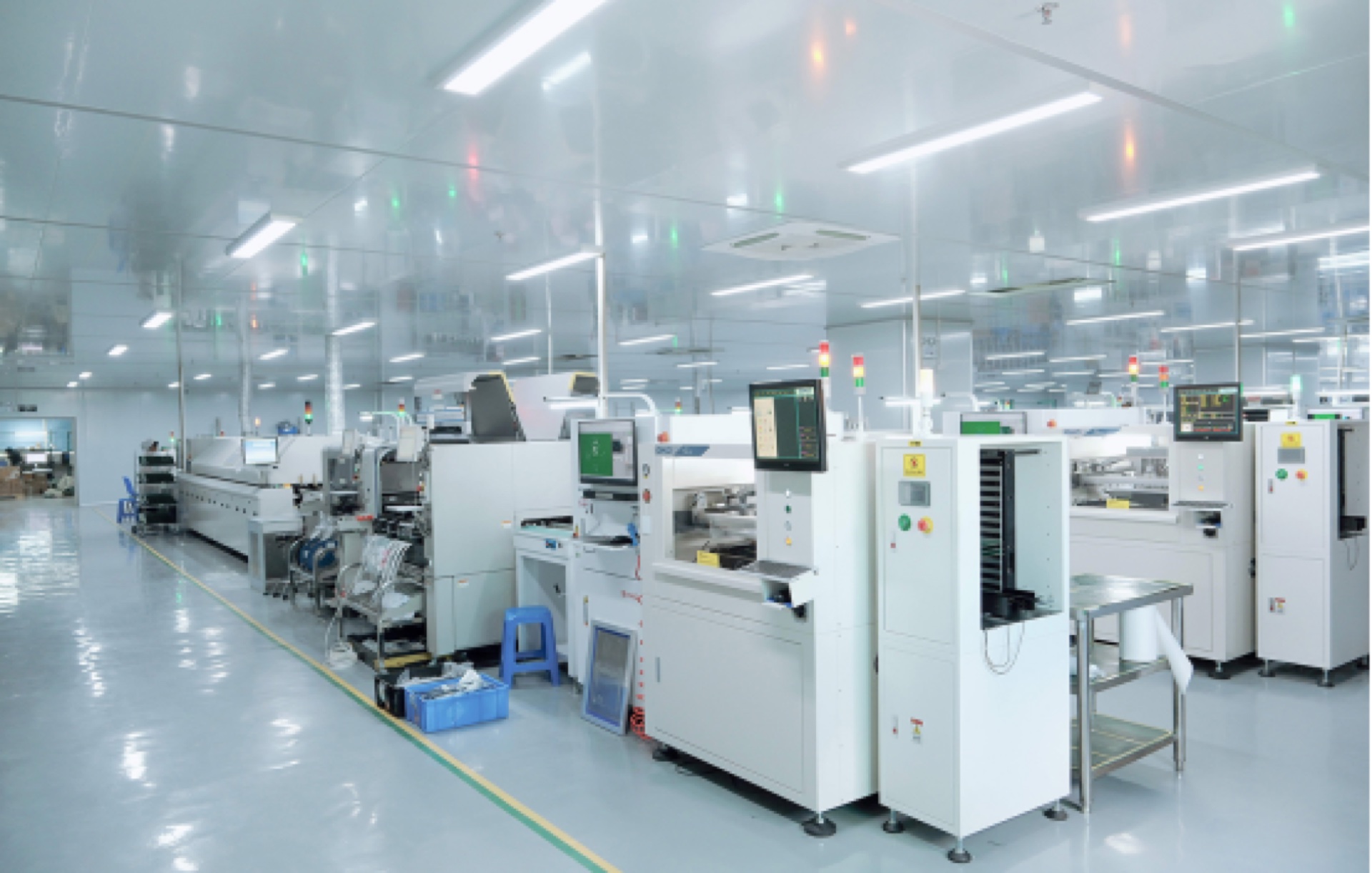
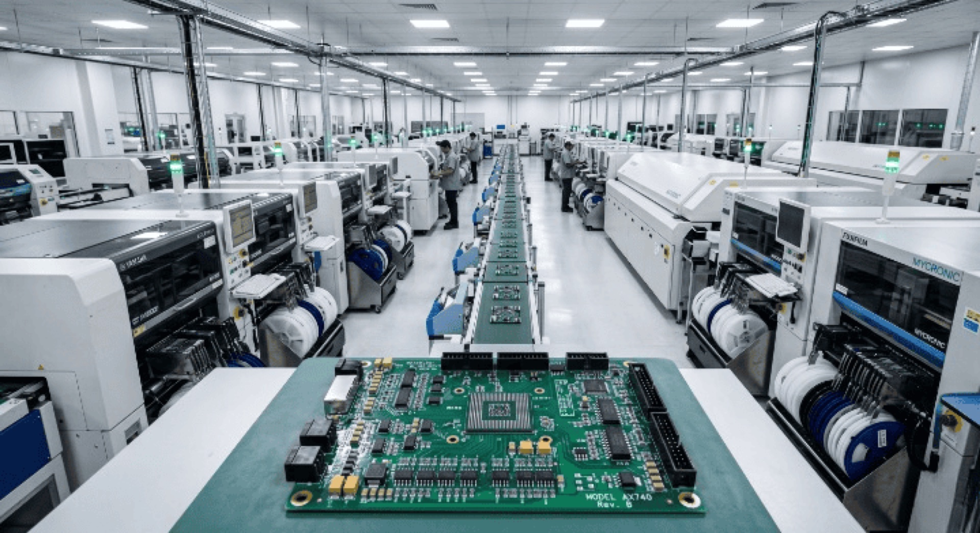
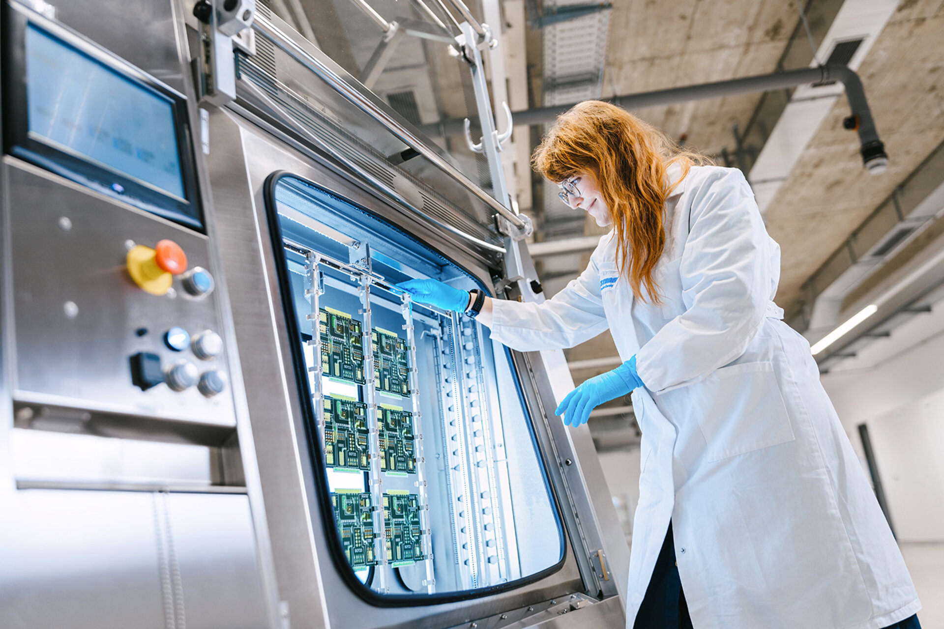
Service Overview
Full-service PCB assembly (SMT + DIP) through final assembly and testing. Ideal for small-to-mid production runs (100–10,000 units).
Process Flow
- Component sourcing: Bulk procurement via partner trading companies, per BOM
- SMT: Yamaha YSM20 + Fuji NXT III lines
- DIP: Hand insertion + auto-insert
- Reflow / wave soldering: Lead-free
- AOI / X-ray inspection: Solder joint quality
- ICT / FCT: Electrical testing
- Final assembly: Housing + cable harness
- Pre-shipment QC: 24-hour burn-in
Assembly Capability
- Board size: 50 × 50 mm – 350 × 250 mm
- Component size: from 01005 (0.4 × 0.2 mm)
- BGA / QFN / CSP supported
- Double-sided / up to 8-layer boards
Certifications
- ISO 9001
- IPC-A-610 Class 2 / Class 3
- UL certification support (on request)
Request a quote for this product
Contact Us